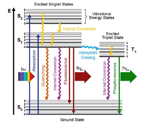
Jablonski Energy Diagram
Above bandgap photoexcitation of semiconductors generates electron-hole pairs. Depending on their binding energy, these can be directly formed as free electrons in conduction band and holes in valence band (the case of most bulk inorganic semiconductors); or remain bound to form neutral quasi particles, excitons (the case of most organic materials). A general photophysical picture of transitions in organic semiconductor upon photoexcitation can be seen from the Jablonski diagram of a single molecule.

Figure 1. Jablonski energy diagram of electronic and vibrational energy levels of an excited molecule.
You can see different photophysical processes that occur at different time.
(i) Absorption: Light absorption is a typical inter-band transitions by which photons with energy above the (optical) band gap are absorbed by the molecule and excite electrons from lower to higher energy levels. Subjected to optical excitation, electrons can either be promoted to the first excited state (S1 state) or to higher states (Sn states). Only transitions between singlet states are allowed due to the conservation of total spin number (ΔS=0).
(ii) Relaxation: A molecule in the excited state may return to the ground state via radiative or non-radiative transitions. The non-radiative vibrational relaxation is very fast phenomena and it usually takes place within the first 100 fs after excitation, while fluorescence is a slower process. Fluorescence is a radiative relaxation process arising from exciton relaxation from excited to ground state, also known as exciton radiative recombination or radiative quenching of excitons. According to Kasha’s rule, once excited the electron energetically relax to the bottom of the excited state (mostly S1 state) within several femtoseconds(fs) or picoseconds(ps), and emission occurs from the bottom of the S1 state to different vibrational levels in the ground state. In other word, fluorescence can only take place from the lowest vibrational level of first excited singlet state S1 to any vibrational level in ground-state S0 and due to this reason, it is slower compared to non-radiative vibrational relaxation. Note that the non-radiative relaxation from S1 to S0 and internal conversion from Sn to S1 via vibrational levels (in the form of heat).
(iii) Photoinduced absorption of excitons: Once excited, electrons in the excited state can be further promoted to higher excited states before relaxation; or they can undergo a non-radiative intersystem crossing process from S1 state to triplet state (T1), resulting in PIA from T1 state to higher triplet states. The relaxation from T1 state to ground state (S0) (phosphorescence) is manifested at much longer lifetimes as compared to fluorescence. The photoluminescence efficiency is defined as the number of emitted photons to the number of absorbed photons and it is independent of the pump intensity. Transferring to T1 reduces the photoluminescence efficiency because transition from T1 to ground state is optically forbidden.
A variety of ultrafast characterization techniques will be used to study excited states in semiconductors, including transient absorption, photoluminescence, and photocurrent.
Transient Absorption: Ultrafast transient absorption is a spectroscopy technique has been developed to study dynamics and evolution of excited states on the sub-picosecond timescales in different materials (i.e. inorganic semiconductors, organic compounds, and biological systems). This technique is a non-contact measurement for carriers that can be generated in the absence of an external electric field. Moreover, this technique has widely been used for studying the highly resistive materials since it is difficult to inject carriers from metal contacts into the materials.
Photoluminescence: Time-resolved photoluminescence (TR-PL), on the other hand, is a powerful technique to probe carrier dynamics and their relaxation pathways in semiconductor nanostructures. Through monitoring the PL decay dynamics of nanostructure emission wavelengths, information on the radiative and non-radiative recombination rates could be extracted.
Photoconductivity: Photoconductivity measurements provide direct evidence of carrier transport upon photogeneration. The magnitude of the conductivity change induced by irradiation depends upon the number of carriers produced per absorbed photon (carrier generation quantum yield) and the mobility of photogenerated carriers. The duration of this change depends upon many factors, such as the lifetime of the carriers and the time for the carriers to encounter a trap. The signatures of charge transfer are manifested in photoconductivity measurements by an increase of photoconductivity and of carrier lifetime by several order of magnitudes.